300MHz to 450MHz Low-Power,
Crystal-Based +10dBm ASK/FSK Transmitter
_______________________________________________________________________________________ 7
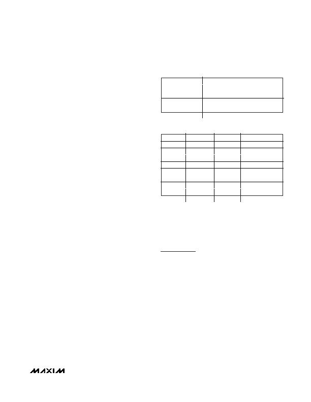
Clock Output
The MAX1479 has a dedicated digital output pin for the
frequency-divided crystal clock signal. This is to be
used as the time base for a microprocessor. The fre-
quency-division ratio is programmable through two dig-
ital input pins (CLK0, CLK1), and is defined in Table 1.
The clock output is designed to drive a 3.5MHz CMOS
rail-to-rail signal into a 10pF capacitive load.
Envelope-Shaping Resistor
The envelope-shaping resistor allows for a gentle turn-
on/turn-off of the PA in ASK mode. This results in a small-
er spectral width of the modulated PA output signal.
Phase-Locked Loop
The PLL block contains a phase detector, charge
pump, integrated loop filter, VCO, asynchronous 32x
clock divider, and crystal oscillator. The PLL requires
no external components. The relationship between the
carrier and crystal frequency is given by:
f
XTAL
= f
RF
/32
Crystal Oscillator
The crystal oscillator in the MAX1479 is designed to
present a capacitance of approximately 3pF to ground
from the XTAL1 and XTAL2 pins in ASK mode. In most
cases, this corresponds to a 4.5pF load capacitance
applied to the external crystal when typical PCB para-
sitics are added. In FSK mode, a percentage (defined
by bits DEV0 to DEV2) of the 3pF internal crystal oscil-
lator capacitance is removed for a logic 1 on the DIN
pin to pull the transmit frequency. The frequency devia-
tion is shown in Table 2. It is very important to use a
crystal with a load capacitance that is equal to the
capacitance of the MAX1479 crystal oscillator plus
PCB parasitics. If very large FSK frequency deviations
are desired, use a crystal with a larger motional capaci-
tance and/or reduce PCB parasitic capacitances.
Power Amplifier
The PA of the MAX1479 is a high-efficiency, open-drain,
switch-mode amplifier. With a proper output-matching
network, the PA can drive a wide range of impedances,
including small-loop PCB trace antennas and any 50?/DIV>
antennas. The output-matching network for a 50?anten-
na is shown in the Typical Application Circuit. The out-
put-matching network suppresses the carrier harmonics
and transforms the antenna impedance to an optimal
impedance at PAOUT (pin 8), which is about 250?
When the output-matching network is properly tuned,
the power amplifier is highly efficient. The Typical
Application Circuit delivers +10dBm at a supply volt-
age of +2.7V, and draws a supply current of 6.7mA for
ASK/OOK operation (V
DIN
at 50% duty cycle) and
10.5mA for FSK operation. Thus, the overall efficiency
at 100% duty cycle is 35%. The efficiency of the power
amplifier itself is about 50%. An external resistor at
ROUT sets the output power.
Applications Information
Output Matching to 50?/DIV>
When matched to a 50?system, the MAX1479 PA is
capable of delivering more than +10dBm of output
power at V
DD
= 2.7V. The output of the PA is an open-
drain transistor that requires external impedance
matching and pullup inductance for proper biasing.
The pullup inductance from PAOUT to V
DD
serves three
main purposes: It forms a resonant tank circuit with the
capacitance of the PA output, provides biasing for the
PA, and becomes a high-frequency choke to reduce
the RF energy coupling into V
DD
. Maximum efficiency is
achieved when the PA drives a load of 250? The rec-
ommended output-matching network topology is shown
in the Typical Application Circuit.
CLK1
CLK0
CLKOUT
0
0
Logic 0
0
1
F
XTAL
/4
1
0
F
XTAL
/8
1
1
f
XTAL
/16
Table 1. Clock Divider Settings
DEV2
DEV1
DEV0
DEVIATION
0
0
0
1/8 x max
0
0
1
1/4 x max
0
1
0
3/8 x max
0
1
1
1/2 x max
1
0
0
5/8 x max
1
0
1
3/4 x max
1
1
0
7/8 x max
1
1
1
Max
Table 2. Frequency-Deviation Settings
发布紧急采购,3分钟左右您将得到回复。
相关PDF资料
MAX19790ETX+T
IC 250MHZ - 4GHZ VAR ATTEN
MAX19792ETX+
ATTENUATR 46DB 50OHM 4GHZ 36TQFN
MAX19794ETX+
ATTENUATR 46DB 50OHM 4GHZ 36TQFN
MAX2365ETM+T
IC TRANSMITTER QUAD 48TQFN-EP
MAX2369EGM+TD
IC TRANSMITTER QUAD 48QFN-EP
MAX2850ITK+
TRANSMITTER MIMO 5GHZ 4CH 68TQFN
MAX7057ASE+T
IC TRANSMITTER ASK/FSK 16-SOIC
MBA-2060
ANTENNA METROLOGY BICONICAL
相关代理商/技术参数
MAX1479ATE-T
功能描述:射频发射器 RoHS:否 制造商:Micrel 类型:ASK Transmitter 封装 / 箱体:SOT-23-6 工作频率:300 MHz to 450 MHz 封装:Reel
MAX1479EVKIT-315
功能描述:射频开发工具 MAX1479 Eval Kit RoHS:否 制造商:Taiyo Yuden 产品:Wireless Modules 类型:Wireless Audio 工具用于评估:WYSAAVDX7 频率: 工作电源电压:3.4 V to 5.5 V
MAX1479EVKIT-433
功能描述:射频开发工具 MAX1479 Eval Kit RoHS:否 制造商:Taiyo Yuden 产品:Wireless Modules 类型:Wireless Audio 工具用于评估:WYSAAVDX7 频率: 工作电源电压:3.4 V to 5.5 V
MAX147ACAP
功能描述:模数转换器 - ADC RoHS:否 制造商:Texas Instruments 通道数量:2 结构:Sigma-Delta 转换速率:125 SPs to 8 KSPs 分辨率:24 bit 输入类型:Differential 信噪比:107 dB 接口类型:SPI 工作电源电压:1.7 V to 3.6 V, 2.7 V to 5.25 V 最大工作温度:+ 85 C 安装风格:SMD/SMT 封装 / 箱体:VQFN-32
MAX147ACAP+
功能描述:模数转换器 - ADC 12-Bit 8Ch 133ksps 5.25V Precision ADC RoHS:否 制造商:Texas Instruments 通道数量:2 结构:Sigma-Delta 转换速率:125 SPs to 8 KSPs 分辨率:24 bit 输入类型:Differential 信噪比:107 dB 接口类型:SPI 工作电源电压:1.7 V to 3.6 V, 2.7 V to 5.25 V 最大工作温度:+ 85 C 安装风格:SMD/SMT 封装 / 箱体:VQFN-32
MAX147ACAP+T
功能描述:模数转换器 - ADC 12-Bit 8Ch 133ksps 5.25V Precision ADC RoHS:否 制造商:Texas Instruments 通道数量:2 结构:Sigma-Delta 转换速率:125 SPs to 8 KSPs 分辨率:24 bit 输入类型:Differential 信噪比:107 dB 接口类型:SPI 工作电源电压:1.7 V to 3.6 V, 2.7 V to 5.25 V 最大工作温度:+ 85 C 安装风格:SMD/SMT 封装 / 箱体:VQFN-32
MAX147ACAP-T
功能描述:模数转换器 - ADC RoHS:否 制造商:Texas Instruments 通道数量:2 结构:Sigma-Delta 转换速率:125 SPs to 8 KSPs 分辨率:24 bit 输入类型:Differential 信噪比:107 dB 接口类型:SPI 工作电源电压:1.7 V to 3.6 V, 2.7 V to 5.25 V 最大工作温度:+ 85 C 安装风格:SMD/SMT 封装 / 箱体:VQFN-32
MAX147ACPP
功能描述:模数转换器 - ADC RoHS:否 制造商:Texas Instruments 通道数量:2 结构:Sigma-Delta 转换速率:125 SPs to 8 KSPs 分辨率:24 bit 输入类型:Differential 信噪比:107 dB 接口类型:SPI 工作电源电压:1.7 V to 3.6 V, 2.7 V to 5.25 V 最大工作温度:+ 85 C 安装风格:SMD/SMT 封装 / 箱体:VQFN-32